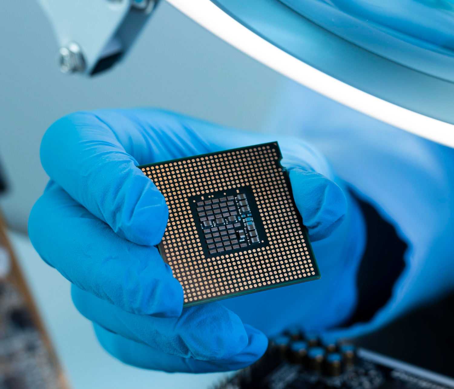
 In the evolution of semiconductor manufacturing, advanced lithography processes rely heavily on key materials like photomasks and photoresists to achieve smaller, more powerful devices. Erik Hosler emphasizes the importance of these materials as lithography techniques, such as Extreme Ultraviolet (EUV), evolve to meet the industry’s demand for higher precision. These materials enable manufacturers to create faster, more efficient chips for devices ranging from smartphones to supercomputers, making them a crucial element of semiconductor innovation.
The Role of Photomasks in Precision Manufacturing
Photomasks serve as the blueprint in semiconductor production, carrying intricate circuit patterns that must be transferred onto silicon wafers. These masks ensure every detail of the circuit is accurately represented. As semiconductor nodes have shrunk below 7 nanometers (nm), photomask precision has become more critical. The materials used in photomasks must withstand repeated exposure to EUV light without degrading, ensuring reliable patterning and consistent results in high-volume manufacturing. Photomasks must also remain durable against environmental factors such as temperature fluctuations and chemical exposure to maintain long-term stability and efficiency.
Photoresists: Enabling Extreme Precision
Equally important are photoresists, light-sensitive materials that react to EUV or ultraviolet (UV) light exposure to transfer circuit patterns from the photomask onto the wafer. These materials are essential for maintaining design integrity at such small scales.
Erik Hosler explains the potential of EUV lithography: “Power-driven performance changes for EUV open the door for a ‘final era’ of lithography tooling, enabling the creation of features smaller than 10 nm.” This highlights the role of advanced materials like photoresists in pushing the boundaries of semiconductor manufacturing. Modern photoresists are being engineered to reduce defects and improve performance, ensuring that each wafer produced meets the high standards of today’s electronics industry.
Supporting Materials for Advanced Lithography
Beyond photomasks and photoresists, anti-reflective coatings (ARCs) and metrology tools play key roles in advanced lithography. ARCs prevent distortions caused by reflections, improving the accuracy of the patterning process. Metrology tools inspect and measure the precision of each pattern, ensuring any imperfections are detected and corrected before mass production, which is crucial for maintaining high-quality chips.
Advancing Lithography: The Next Generation of Materials
As semiconductor technology continues to evolve, refining materials such as photomasks, photoresists, and ARCs will drive innovation in high-performance computing (HPC) and artificial intelligence (AI). By pushing the limits of these materials, the semiconductor industry will unlock new possibilities in chip design, ensuring faster, smaller, and more efficient devices for future technologies.


